
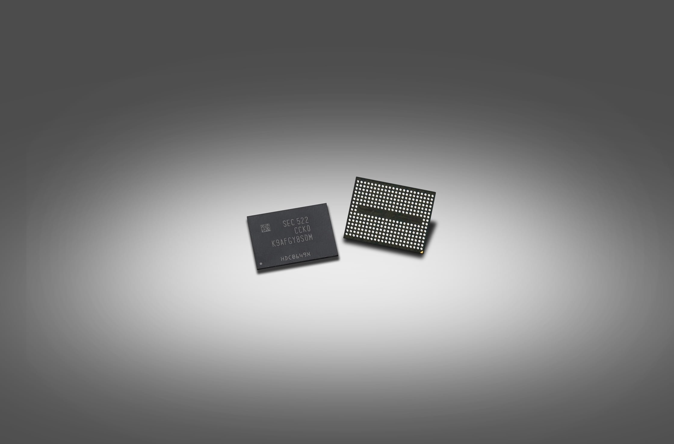
Samsung Electronics Begins Mass Producing Industry First 256-Gigabit, 3D V-NAND Flash Memory
Electronics Co., Ltd., the world leader in advanced memory technology, today announced that it has begun mass producing the industry’s first 256-gigabit (Gb), three-dimensional (3D) Vertical NAND (V-NAND) flash memory based on 48 layers of 3-bit multi-level-cell (MLC) arrays for use in solid state drives (SSDs).
“With the introduction of our 3rd generation V-NAND flash memory to the global market, we can now provide the best-advanced memory solutions, with even higher efficiency based on improved performance, power utilization and manufacturing productivity, thereby accelerating growth of the high-performance and the high-density SSD markets,” said Young-Hyun Jun, President of the Memory Business at Samsung Electronics. “By making full use of Samsung V-NAND’s excellent features, we will expand our premium-level business in the enterprise and data center market segments, as well as in the consumer market, while continuing to strengthen our strategic SSD focus.”
Samsung’s new 256Gb 3D V-NAND flash doubles the density of conventional 128Gb NAND flash chips. In addition to enabling 32 gigabytes (256 gigabits) of memory storage on a single die, the new chip will also easily double the capacity of Samsung’s existing SSD line-ups and provide an ideal solution for multi-terabyte SSDs.
Samsung introduced its 2nd generation V-NAND (32-layer 3-bit MLC V-NAND) chips in August 2014, and launched its 3rd generation V-NAND (48-layer 3-bit MLC V-NAND) chips in just one year, in continuing to lead the 3D memory era.
In the new V-NAND chip, each cell utilizes the same 3D Charge Trap Flash (CTF) structure in which the cell arrays are stacked vertically to form a 48-storied mass that is electrically connected through some 1.8 billion channel holes punching through the arrays thanks to a special etching technology. In total, each chip contains over 85.3 billion cells. They each can store 3 bits of data, resulting 256 billion bits of data, in other words, 256Gb on a chip no larger than the tip of a finger.
A 48-layer 3-bit MLC 256Gb V-NAND flash chip consumes over a 30 percent reduction in power compared to a 32-layer, 3-bit MLC, 128Gb V-NAND chip when storing the same amount of data. During production, the new chip also achieves approximately 40 percent more productivity over its 32-layer predecessor, bringing much-enhanced cost competitiveness to the SSD market, while mainly utilizing existing equipment.
Samsung plans to produce 3rd generation V-NAND throughout the remainder of 2015, to enable more accelerated adoption of terabyte-level SSDs. While now introducing SSDs with densities of two terabytes and above for consumers, Samsung also plans to increase its high-density SSD sales for the enterprise and data center storage markets with leading-edge PCIe NVMe and SAS interfaces.


